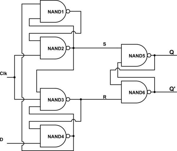
Positive Edge Triggered D Flip Flop Circuit Diagram

Roy

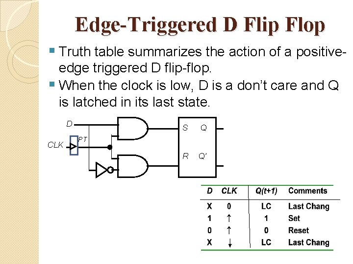
Let's analyze it for each clock edge. It is commonly used as a basic building block in digital. Timing diagram assume that q is initially zero for this problem. The positive edge d type flip flop, which changes its o/p according to the i/p with the +ve transition of the clock pulse.

D Positive Edge Triggered Flip Flop With T Flip Flop Calgarylasopa

D positive edge triggered flip flop with t flip flop calgarylasopa

Then we study the timing diagram of the circuit in dsch and compare it with an ideal circuit timing diagram. Web in this paper, we investigate single electron encoded logic (seel) memory circuits, in which the boolean logic values are encoded as zero or one electron charges. Scan chains testing for latches to reduce area and.

The Output Was Initially Zero (Or To Be Precise, High Impedance).

Web rising edge triggered d flip flop | positive edge d flip flop. This generated timing diagram is shown in.

Electronic How is the Truth Table of Positive edge triggered D Flip
praxe pilulka rytmus positive edge triggered d flip flop truth table
CircuitVerse A positiveedgetriggered D flipflop
Solved QUESTION 1 Referring to the positiveedge triggered D
Examples
Examples
D positive edge triggered flip flop with t flip flop calgarylasopa
PPT EENG 2710 Chapter 6 PowerPoint Presentation, free download ID
Electronic CMOS implementation of D flipflop Valuable Tech Notes

SEARCH


YOU MIGHT ALSO LIKE